proper strain relief in flex pcb board assemblies
As a flexible PCB board endures mechanical strains beyond those experienced by rigid PCBs, engineers must take unique precautions to avoid conductor cracking and delamination. These engineering practices ensure flex circuits deliver reliable performance across diverse applications and environments. To minimize z-axis delamination risks, flex PCBs should minimize the number of layers where rigid materials meet flex circuitry. Each interface adds a potential stress point that can lead to delamination.
To improve handling, flex PCBs use stiffening films and bars that stabilize areas that require precise alignment like connectors. Stiffeners can also prevent bending stresses from damaging copper traces and solder joints. The amount of flex a pcb can handle depends on its stack-up, copper trace thickness, and the amount of rigidity built into the circuit. The required bending radius must be specified in the flex section of the board during the CAD phase. Using a larger bending radius reduces the number of conductors exposed to damage and improves flex lifetime.
Creating a flex pcb board with the right stack-up and calculating the correct bending radius will make your design more resilient against mechanical stress. It will also reduce the likelihood of damage to critical components during assembly and testing.
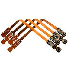
How do you ensure proper strain relief in flex pcb board assemblies?
In addition to identifying the flex section bending radius, designers should identify the minimum amount of flex that can be routed without causing damage to the copper circuitry. The optimum bending radius can be determined by measuring the distance between the neutral bend axis and the edge of the conductor. This measurement can be done by using a ruler or caliper and a protractor.
If you have a tight bending radius, you can optimize your design by selecting the right layer thickness and by making your copper traces thinner. However, keep in mind that this will also affect the conductor’s impedance and signal transmission.
Another way to increase flex pcb bending capabilities is by adding slack loops on the ends of the flex circuit. This will allow the slack loop to absorb stress when bending instead of propagating it through fragile solder joints. Despite their many advantages, designing and manufacturing flex PCBs come with challenges. The materials and processes involved can be more expensive than those for rigid PCBs. Design engineers must carefully consider factors such as bend radius, flexing frequency, and the potential for stress fractures. Proper design and simulation tools are essential to ensure the reliability and performance of the final product.
To ensure that your flex circuits are assembled in the most secure manner, you can use pressure-sensitive adhesives. These types of adhesives are typically applied to the surface of the bare circuit boards before they are assembled into the finished product. These adhesives can withstand high reflow temperatures and can help a flex pcb withstand high-speed flexing. These adhesives can also help in preventing the formation of air bubbles between the rigid and flex sections of the pcb. This will ensure that the flex circuits do not separate after the assembly and reflow process.